


Advanced semiconductor packaging refers to the methods and technologies used to encapsulate semiconductor chips in a protective yet efficient manner that allows them to function optimally within electronic devices. As the demand for smaller, faster, and more efficient electronics continues to grow, so does the need for more sophisticated packaging methods. This process goes beyond traditional packaging techniques by focusing on performance, miniaturization, and thermal management while also reducing the size and cost of electronic devices.
Why Advanced Semiconductor Packaging is Crucial
With the growing complexity of modern integrated circuits (ICs), traditional packaging methods are often inadequate. Advanced semiconductor packaging enables devices to meet increasing performance demands while managing factors like heat dissipation, signal integrity, and mechanical stress. These innovations are crucial for industries ranging from consumer electronics to automotive applications.
Types of Advanced Semiconductor Packaging
Several different methods are employed in advanced semiconductor packaging, each with unique advantages depending on the specific requirements of the device. Some of the most prominent techniques include:
1. System-in-Package (SiP)
In a SiP design, multiple chips are integrated into a single package. This packaging method is especially beneficial for complex systems that require a combination of different ICs, such as sensors, processors, and memory units, to work together within a compact form factor. This approach reduces the overall space needed for the device, making it ideal for mobile devices and wearable technologies.
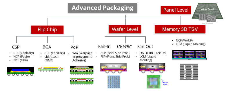
2. Ball Grid Array (BGA)
BGA is one of the most commonly used packaging techniques in modern electronics. This method involves placing an array of solder balls underneath the chip for better heat dissipation, electrical conductivity, and more reliable connections. It is widely used in applications such as computers, mobile phones, and automotive electronics.
3. Flip-Chip Packaging
Flip-chip packaging is a process where the semiconductor die is flipped over so that the active side of the chip faces downward toward the package. This eliminates the need for bonding wires and allows for improved signal integrity and better thermal management. Flip-chip technology is increasingly being used in high-performance computing and telecommunications equipment.
4. 3D Packaging
As the demand for miniaturized electronics grows, 3D semiconductor packaging has emerged as a cutting-edge solution. This technique stacks multiple ICs vertically, enabling higher-density packaging with better performance and reduced size. The use of advanced interconnects and through-silicon vias (TSVs) makes 3D packaging suitable for applications that require high-speed processing and memory.
Key Challenges in Advanced Semiconductor Packaging
Despite the advantages of advanced semiconductor packaging, there are several challenges that need to be addressed to ensure that the packaging process is effective and efficient:
1. Heat Management
As semiconductors become more powerful, they also generate more heat. Effective heat dissipation techniques are crucial for preventing overheating and ensuring that devices perform optimally. Advanced semiconductor packaging technologies incorporate materials and designs that help manage heat, such as using heat sinks, thermal vias, and specialized packaging materials.
2. Miniaturization vs. Reliability
As the industry continues to push toward smaller devices with higher performance, manufacturers must balance miniaturization with reliability. Ensuring that smaller devices remain robust and durable is key to their long-term performance in various applications, from smartphones to automotive sensors.
3. Signal Integrity and Interference
Signal integrity is essential for maintaining the performance of electronic devices, particularly as operating speeds increase. Advanced packaging designs must minimize signal loss and interference to ensure that high-frequency signals can be transmitted effectively without degradation.
Chengliankaida Technology's Role in Advanced Semiconductor Packaging
Chengliankaida Technology has made significant strides in advanced semiconductor packaging, especially in power devices. By focusing on vacuum welding machines and production lines for semiconductor device packaging, the company has played an essential role in solving issues related to void rates and hermetic packaging.
Vacuum Welding for Precision Packaging
Chengliankaida’s vacuum welding technology provides a solution to the challenge of creating hermetic seals for power devices. This process ensures that devices are sealed tightly, protecting them from environmental factors such as moisture and dust, which could compromise their performance. This is particularly important for power electronics that operate under extreme conditions.
Collaborations and Innovations
Chengliankaida Technology has partnered with the IGBT (Insulated Gate Bipolar Transistor) industry alliance and various academic institutions to stay at the forefront of advanced semiconductor packaging developments. The company's R&D center plays a critical role in advancing packaging technology for power devices, providing high-quality solutions for industries ranging from renewable energy to automotive.
Future Trends in Advanced Semiconductor Packaging
The future of advanced semiconductor packaging is closely tied to the continued advancements in chip design, manufacturing, and materials science. Some key trends expected to shape the industry include:
1. Advanced Materials
The development of new materials, such as high-performance polymers and ceramics, will improve the efficiency and reliability of semiconductor packaging. These materials will help in managing heat more effectively and will also contribute to reducing the overall size and weight of electronic devices.
2. Artificial Intelligence in Packaging
AI and machine learning are increasingly being used to optimize semiconductor packaging processes. These technologies can help predict potential issues in packaging design, ensuring that defects are caught early in the production process.
3. Integration of Multiple Functions
As consumer demand for multifunctional devices grows, packaging solutions will need to integrate more functions into smaller spaces. This will include combining memory, processing power, and sensing capabilities within a single package.
Conclusion
Advanced semiconductor packaging is a critical part of the development of modern electronic devices, enabling the miniaturization and enhanced performance required in today's fast-paced technology market. Chengliankaida Technology’s expertise in vacuum welding and its focus on continuous innovation has positioned it as a leader in this field, addressing key challenges such as void rates and hermetic packaging. As the demand for more advanced, compact, and efficient electronics continues to rise, advanced semiconductor packaging will play an even more significant role in shaping the future of the electronics industry.
Comments